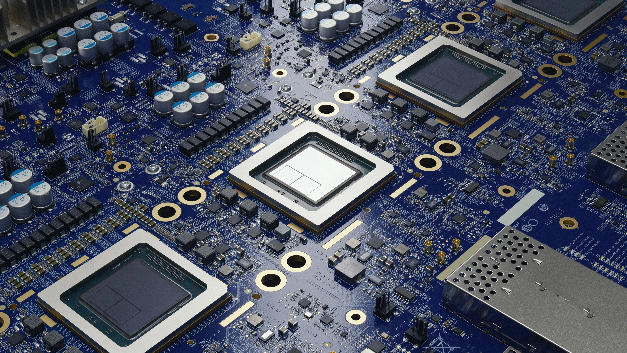
एक modern semiconductor chip को design करना किसी एक circuit को draw करने जैसा काम नहीं है। एक बड़े processor में करोड़ों या उससे भी अधिक transistors, memory blocks, interconnects और अलग-अलग functional units होते हैं। हर हिस्से को इस तरह arrange करना पड़ता है कि chip पर्याप्त तेज चले, कम power इस्तेमाल करे और silicon पर बहुत ज्यादा जगह भी न घेरे।
यहीं एक दिलचस्प बदलाव हो रहा है। AI अब सिर्फ chips पर चल नहीं रहा, बल्कि chip design की प्रक्रिया में भी इस्तेमाल हो रहा है। यानी जिस technology के लिए नई generations के processors बनाए जा रहे हैं, वही technology उन processors को बेहतर बनाने में engineers की मदद भी कर रही है।
इसी approach को AI-driven chip design कहा जाता है। इसमें AI को Electronic Design Automation यानी EDA tools के साथ जोड़ा जाता है, ताकि design के ऐसे विकल्प खोजे जा सकें जिन्हें इंसान manually explore करने में बहुत अधिक समय लगा सकता है। Reinforcement learning, generative AI और AI agents इस बदलाव के अलग-अलग हिस्से हैं।
AI-driven chip design क्या है?
सबसे पहले एक जरूरी फर्क समझना चाहिए। AI chip design और AI-driven chip design एक ही चीज नहीं हैं।
AI chip design का मतलब है ऐसा hardware बनाना जो AI workloads को तेजी से चलाए। GPU, NPU और AI-focused ASIC इसके उदाहरण हैं। दूसरी तरफ AI-driven chip design का अर्थ है AI का इस्तेमाल खुद semiconductor design process को बेहतर बनाने में करना।
इस प्रक्रिया में AI किसी engineer की जगह बैठकर एक button दबाते ही पूरा commercial processor तैयार नहीं कर देता। बल्कि यह EDA software के साथ काम करके बहुत बड़े design space में संभावित solutions खोज सकता है, simulation results से सीख सकता है और कुछ repetitive या optimization-heavy tasks को automate कर सकता है।
Chip design इतना मुश्किल क्यों है?
मान लीजिए किसी chip engineer को एक circuit को तेज बनाना है। वह केवल clock frequency नहीं बढ़ा सकता, क्योंकि इससे power consumption और heat बढ़ सकती है। Area भी सीमित है। इसलिए एक साथ कई लक्ष्य सामने होते हैं:
- Power कम रखना
- Performance बढ़ाना
- Chip का Area नियंत्रित रखना
- Timing requirements पूरा करना
- Manufacturing rules का पालन करना
- Design को सही तरीके से verify करना
इन्हें अक्सर PPA यानी Power, Performance and Area के रूप में देखा जाता है। समस्या यह है कि एक parameter बदलने पर दूसरे parameters प्रभावित हो सकते हैं। किसी design को छोटा करने से routing मुश्किल हो सकती है, performance बढ़ाने से power बढ़ सकती है और power घटाने से speed प्रभावित हो सकती है।
इसलिए chip design एक विशाल optimization problem बन जाता है। AI-driven tools का फायदा इसी search space में दिखाई देता है।
EDA क्या करता है?
Electronic Design Automation यानी EDA उन software tools का पूरा ecosystem है जिनकी मदद से engineers semiconductor chips को design, simulate, verify और तैयार करते हैं। इसमें RTL design, synthesis, placement, routing, timing analysis, verification और testing जैसे कई stages शामिल होते हैं।
सरल भाषा में EDA को chip engineer की digital workshop समझ सकते हैं। Engineer design की requirements और constraints देता है, जबकि EDA tools उस design को अलग-अलग stages से गुजारकर यह जांचते हैं कि वह वास्तविक silicon पर बनाया जा सकता है या नहीं।
AI इस workshop के अंदर एक intelligent optimization layer की तरह काम कर सकता है। वह अलग-अलग settings आजमा सकता है, परिणाम देख सकता है और अगली कोशिश को बेहतर बनाने के लिए previous results का इस्तेमाल कर सकता है।
AI से chip design कैसे होता है?
AI-driven chip design को एक ही algorithm से समझना मुश्किल है। अलग stages में अलग AI techniques उपयोगी हो सकती हैं। तीन approaches खास तौर पर महत्वपूर्ण हैं: Reinforcement Learning, Generative AI और AI Agents।
1. Reinforcement Learning: बार-बार कोशिश करके बेहतर विकल्प खोजना
Reinforcement Learning यानी RL में AI किसी environment में actions लेता है और उनके परिणाम के आधार पर reward प्राप्त करता है। Chip design में environment EDA workflow हो सकता है और reward PPA, timing या दूसरे engineering objectives से जुड़ा हो सकता है।
उदाहरण के लिए AI को किसी chip block की placement optimize करनी है। वह एक arrangement चुनता है, EDA tool उसका performance evaluate करता है और परिणाम के आधार पर AI अगला arrangement चुनता है। हजारों या लाखों संभावित combinations में से बेहतर region खोजने के लिए यह process दोहराया जा सकता है।
यह approach खास तौर पर तब उपयोगी हो सकती है जब problem में बहुत सारे parameters हों और हर combination को manually test करना संभव न हो। Synopsys के अनुसार reinforcement-learning आधारित design-space optimization को physical design जैसे workloads में इस्तेमाल किया जा रहा है।
2. Generative AI: Engineer के साथ संवाद और design tasks
Generative AI का इस्तेमाल chip design में केवल text लिखने के लिए नहीं है। यह engineers को specifications समझने, design information खोजने, code या test-related सामग्री तैयार करने और complex EDA workflows के साथ interaction में सहायता कर सकता है।
उदाहरण के लिए किसी engineer के पास किसी RTL block की specification हो सकती है। Generative AI उस specification से प्रारंभिक RTL या verification-related सामग्री तैयार करने में मदद कर सकता है। लेकिन generated output को सीधे silicon में भेज देना सुरक्षित नहीं होगा। उसे traditional EDA checks और verification से गुजरना जरूरी है।
2026 में Synopsys ने ऐसे agentic workflows प्रदर्शित किए हैं जो natural-language या formal specifications से RTL generation, linting, testbench generation और iterative verification जैसे कई front-end tasks को एक workflow में जोड़ते हैं।
3. AI Agents: अलग-अलग tools को एक workflow में जोड़ना
AI chatbot एक सवाल का जवाब दे सकता है। AI agent उससे आगे जाकर किसी लक्ष्य को पाने के लिए कई steps execute कर सकता है। Chip design में इसका मतलब हो सकता है कि एक agent design specification पढ़े, दूसरा RTL की जांच करे, कोई verification task चलाए और फिर system results के आधार पर अगला कदम तय करे।
इसी वजह से semiconductor industry में agentic AI पर ध्यान बढ़ रहा है। 2026 में Synopsys ने AMD और Microsoft के साथ autonomous EDA workflows की घोषणा की, जबकि industry discussions में design और verification के लिए agentic workflows को तेजी से विकसित होती दिशा बताया गया है।
AI chip के Physical Design में क्या करता है?
Chip design का physical stage विशेष रूप से complex है। यहां logical design को silicon पर वास्तविक physical layout में बदला जाता है। इसमें floorplanning, placement और routing जैसे काम शामिल होते हैं।
मान लीजिए किसी chip में हजारों blocks हैं। इन्हें silicon die पर कहां रखा जाए ताकि signals कम दूरी तय करें, congestion घटे और timing targets पूरे हों? एक छोटी placement change कई दूसरे हिस्सों को प्रभावित कर सकती है।
AI यहां अलग-अलग design configurations explore कर सकता है। Reinforcement learning आधारित systems बार-बार EDA evaluation से feedback लेकर ऐसे combinations खोज सकते हैं जो PPA objectives के करीब हों। Synopsys के अनुसार उसका DSO.ai approach physical-design search space में design choices और workflow parameters को explore करने के लिए AI का इस्तेमाल करता है।
Verification में AI की भूमिका क्यों बढ़ रही है?
Chip बनाना ही पर्याप्त नहीं है। यह साबित करना भी जरूरी है कि chip अपेक्षित तरीके से काम करेगी। बड़े SoC में verification बेहद बड़ा काम हो सकता है क्योंकि अलग-अलग operating conditions और corner cases की संख्या बहुत ज्यादा होती है।
AI verification coverage के gaps खोजने, regression results का analysis करने, test generation में मदद करने और debugging workflow को accelerate करने के लिए इस्तेमाल किया जा सकता है। Synopsys ने 2026 में AI-assisted verification के लिए ऐसे use cases बताए हैं जिनमें functional coverage और test selection जैसे tasks शामिल हैं।
यहां AI का सबसे उपयोगी रूप अक्सर “सब कुछ खुद करने वाला system” नहीं बल्कि ऐसा system है जो engineer को उन हिस्सों पर जल्दी पहुंचने में मदद करे जहां manual investigation की जरूरत है।
क्या AI खुद computer chip का पूरा design कर सकता है?
आज की स्थिति में इसे पूरी तरह autonomous process मानना सही नहीं होगा।
AI कई design tasks को automate या optimize कर सकता है, लेकिन chip architecture, specifications, constraints, verification strategy और final sign-off जैसे महत्वपूर्ण निर्णयों में human engineers की भूमिका बनी हुई है। Semiconductor में छोटी गलती भी costly silicon respin का कारण बन सकती है, इसलिए AI-generated output को independent checks से गुजरना पड़ता है।
2026 की Semiconductor Engineering discussions में भी AI की reliability और “black-box” behavior को लेकर concerns सामने आए हैं। Experts ने human oversight और verification safeguards को महत्वपूर्ण बताया है।
AI से Semiconductor Design करने के क्या फायदे हैं?
बहुत बड़ा design space explore करना
मानव engineers के पास हर possible configuration आजमाने का समय नहीं होता। AI parallel या iterative search के जरिए अधिक विकल्पों को explore कर सकता है।
PPA optimization
Power, Performance और Area के बीच संतुलन ढूंढना chip design की केंद्रीय समस्याओं में से एक है। AI इन objectives के आधार पर promising configurations खोजने में मदद कर सकता है।
Design cycle छोटा करना
यदि repetitive experiments और optimization loops तेजी से पूरे हो जाएं, तो engineering team जल्दी design closure तक पहुंच सकती है। Synopsys ने अपने कुछ AI-driven workflows में design exploration और productivity improvements report किए हैं, हालांकि ये परिणाम specific tools और workloads से जुड़े हैं और हर chip पर समान परिणाम की गारंटी नहीं देते।
Engineers को high-value काम के लिए समय देना
अगर AI हजारों routine configurations को automatically evaluate कर सके, तो engineers अपना समय architecture, trade-offs और नए ideas पर ज्यादा लगा सकते हैं।
इस technology की सीमाएं भी उतनी ही महत्वपूर्ण हैं
AI-driven chip design के सामने सबसे बड़ा सवाल reliability का है। Generative AI गलत RTL, गलत assumption या misleading suggestion दे सकता है। इसलिए semiconductor में सामान्य chatbot-style trust पर्याप्त नहीं है।
दूसरी समस्या proprietary data है। Leading-edge chip companies के पास design databases, process information और internal know-how सार्वजनिक नहीं होते। इसलिए हर problem को खुले internet data पर trained सामान्य AI model से हल नहीं किया जा सकता। कुछ AI approaches proprietary design environment और company-specific data के साथ काम करने के लिए बनाए जा रहे हैं।
तीसरी समस्या explainability है। यदि AI किसी unusual placement या optimization choice को बेहतर बताता है, तो engineer को यह समझना पड़ सकता है कि वह choice क्यों चुनी गई। Silicon design में केवल अच्छा score पर्याप्त नहीं; design को reliable, manufacturable और verifiable भी होना चाहिए।
चौथी चुनौती compute cost है। AI को train या run करने के लिए भी computational resources चाहिए। इसलिए किसी workflow में AI जोड़ने से हमेशा total energy या total cost कम होगी, ऐसा मानना सही नहीं है। फायदा workload और implementation पर निर्भर करता है।
भारत के लिए AI-driven chip design क्यों महत्वपूर्ण है?
भारत का semiconductor ecosystem केवल fabrication तक सीमित नहीं है। Chip design, EDA skills, verification, embedded systems और ASIC development भी इसकी महत्वपूर्ण कड़ियां हैं। SEMICON India के design और EDA कार्यक्रम में भी advanced chip design की complexity, verification और EDA tools के बदलते role पर चर्चा की गई है।
AI-driven EDA भारत के लिए खास तौर पर इसलिए महत्वपूर्ण हो सकता है क्योंकि chip design में skilled engineers की productivity बढ़ाना semiconductor ecosystem के विस्तार के साथ उपयोगी होगा। अगर AI tools design exploration और verification के कुछ repetitive हिस्सों को संभालते हैं, तो छोटी teams भी अधिक complex design workloads पर काम करने में सक्षम हो सकती हैं।
AI-driven chip design का अगला चरण क्या हो सकता है?
अभी AI को chip design के अलग-अलग tasks में लगाया जा रहा है। अगला चरण इन tools को जोड़कर अधिक continuous workflow बनाने का है। Specification से RTL, RTL से verification, verification से physical implementation और फिर PPA optimization तक AI agents के बीच coordination बढ़ सकता है।
यहां “autonomous chip design” शब्द सुनने को मिल सकता है, लेकिन इसे सावधानी से समझना चाहिए। इसका अर्थ जरूरी नहीं कि engineer केवल एक sentence लिखे और कुछ घंटों बाद factory-ready chip मिल जाए। ज्यादा realistic दिशा ऐसी है जिसमें AI कई engineering loops को खुद execute करे, जबकि humans objectives, constraints और approval points नियंत्रित करें।
Synopsys ने 2026 में agentic EDA workflows को design और verification lifecycle में आगे बढ़ाने की घोषणा की है, जबकि semiconductor industry में अन्य कंपनियां भी AI agents और AI-assisted EDA पर काम कर रही हैं।
एक आसान तरीके से पूरी प्रक्रिया समझें
मान लीजिए एक कंपनी कम power वाला नया ASIC बनाना चाहती है। Engineer पहले chip की requirements तय करता है। फिर architecture और RTL तैयार होता है। इसके बाद EDA tools design को synthesize और analyze करते हैं।
यहां AI अलग-अलग जगह काम कर सकता है। Generative AI शुरुआती RTL या verification material तैयार करने में मदद कर सकता है। AI-based verification tools test cases और coverage analysis में सहायता कर सकते हैं। Reinforcement learning physical design में placement और routing के विकल्प खोज सकता है। AI agents इन tasks को एक workflow में जोड़ सकते हैं।
लेकिन अंतिम chip को silicon पर भेजने से पहले design को established verification, timing, power, physical और manufacturing checks से गुजरना होगा। यही वह boundary है जो आज के AI-driven chip design को “AI ने अकेले chip बना दी” जैसी सरल कहानी से अलग करती है।
AI Chip और AI-driven Chip Design में अंतर
| AI Chip | AI-driven Chip Design |
|---|---|
| AI workloads चलाने के लिए hardware बनाया जाता है। | AI का इस्तेमाल hardware design process में किया जाता है। |
| GPU, NPU और AI ASIC इसके उदाहरण हैं। | EDA optimization, verification और agentic workflows इसके उदाहरण हैं। |
| मुख्य लक्ष्य AI computation को efficient बनाना है। | मुख्य लक्ष्य chip development को अधिक efficient और optimized बनाना है। |
निष्कर्ष
AI और semiconductor technology का रिश्ता अब केवल “AI चलाने के लिए बेहतर chip” तक सीमित नहीं है। AI खुद chip design workflow का हिस्सा बन रहा है। EDA tools के अंदर reinforcement learning बड़े design spaces को explore कर सकता है, generative AI engineers के साथ design और verification tasks में सहयोग कर सकता है और AI agents कई tools को एक coordinated workflow में जोड़ सकते हैं।
फिर भी AI अभी chip engineer का पूर्ण विकल्प नहीं है। Semiconductor design में गलती की कीमत बहुत अधिक होती है, इसलिए verification, constraints और human judgment की भूमिका बनी रहेगी। ज्यादा सही तस्वीर एक human-plus-AI engineering workflow की है, जिसमें AI हजारों possibilities को तेजी से खंगालता है और engineer यह तय करता है कि कौन-सा solution वास्तव में सुरक्षित, सही और manufacturable है।
आने वाले वर्षों में semiconductor industry में असली बदलाव शायद यह नहीं होगा कि “AI ने chip बना दी”, बल्कि यह कि एक engineer और AI मिलकर जितने design विकल्प पहले महीनों में explore करते थे, उन्हें कहीं ज्यादा तेजी से evaluate कर सकेंगे। यही AI-driven chip design की सबसे व्यावहारिक और महत्वपूर्ण संभावना है।
FAQ
क्या AI खुद chip design कर सकता है?
AI chip design के कई हिस्सों को automate और optimize कर सकता है, लेकिन वर्तमान technology में पूरी commercial chip को बिना human engineers और independent verification के तैयार करना सामान्य practice नहीं है।
AI chip design में कैसे मदद करता है?
AI design-space exploration, physical design optimization, verification, test generation, regression analysis और कुछ RTL-related tasks में सहायता कर सकता है। कौन-सा AI method उपयोग होगा, यह design stage और problem पर निर्भर करता है।
AI से semiconductor design कैसे किया जाता है?
AI को EDA workflow के साथ जोड़ा जाता है। Reinforcement learning अलग-अलग design configurations को evaluate करके बेहतर विकल्प खोज सकता है, जबकि generative AI और AI agents design तथा verification workflow में engineers की सहायता कर सकते हैं।
AI-driven chip design और AI chip में क्या अंतर है?
AI chip वह hardware है जो AI workloads को चलाने के लिए बनाया जाता है। AI-driven chip design में AI technology का इस्तेमाल उस hardware को design, verify और optimize करने की प्रक्रिया में किया जाता है।
AI chip design में EDA का क्या काम है?
EDA tools chip development के विभिन्न engineering stages को automate और analyze करते हैं। AI इन्हीं tools के ऊपर optimization और automation की अतिरिक्त क्षमता दे सकता है।